Department of Electronics Engg. w/s in VLSI Design & Technology
Overview
B.Tech in Electronics Engineering with Specialization in VLSI Design & Technology
The proliferation of digital economy and consumer electronics has increased the demand for integrated chips and sensors exponentially. Meeting this burgeoning domestic demand is very challenging. Currently, India is importing integrated chips in billions of US dollar. Post-COVID global semiconductor market has grown exponentially with $590 billion in 2021 and also expected to grow to $1 Trillon by 2030. The driving force of this tremendous growth is the technologies such as Artificial Intelligence(AI), Electric Vehicle (EV), 5G Networks, Internet of Things (IoT), Health Care etc. Realization of these technologies, depend on the production of silicon chip for the hardware is required. Many chip-making industries in R&D, design, manufacturing, testing, etc. are established to fill the gap in the chip supply chain. In fact, overall semiconductor import has surpassed that of gold, standing second only to the crude oil. From a long-term economic perspective, the deficit is expected to rise further. Hence, the existing gap must be bridged by realizing indigenous manufacturing of integrated chips.
Most of the tape-out is being siliconized in foreign countries since India has only single Integrated Design to Manufacturing (IDM) pilot line at Semi-Conductor Laboratory (SCL), Chandigarh based on 180nm Node. Recently, Govt. of India (GoI) has given impetus to the Electronics System Design & Manufacturing (ESDM) policy for full flow / custom design (Front-end and Back-end) solution. Foundries and companies are encouraged to set-up chip manufacturing unit under GOI’s Indian semiconductor mission to build vibrant ecosystems of Semiconductor and display systems. However, one of the common concerns associated with setting up and running a commercial fab in India is availability of trained manpower required to run the system.
A serious crunch is observed in the trained manpower in every aspect of semiconductor ecosystem in the country. The various schemes and policies are framed by Govt. of India to encourage start-ups, MSMEs, industries and large business houses. Also, Chips to Startup (C2S) programme of Ministry of Electronics and Information Technology (Meity), Govt. of India. It has been estimated that total manpower requirement over the period of next five to seven years will be around 85,000 at Levels of B. Tech, M.Tech and Ph.Ds in the field of VLSI Technology, Semiconductor Manufacturing, Electronics, Electrical, Mechanical and Chemical Engineering streams. Government of India announced Semiconductor scheme with an outlay of Rs 76,000 Crore in December 2021 to fulfil Aatma Nirbhar Bharath to contribute significantly to the global semiconductor market.
The Government of India is pursuing the National Semiconductor Mission (NSM) to establish a Semiconductor ecosystem in India. MSAJCE is dedicated to becoming a part of this endeavor to create the human resources required for the semiconductor industry in the upcoming years with trained engineers. The outcome of this program is to improve the world through transformative education and impactful research by producing outstanding graduates who are knowledgeable, creative, and passionate about building a vibrant semiconductor and display ecosystem to enable India’s emergence as a global hub for electronics manufacturing and design.
B.Tech in Electronics Engineering with specialization in VLSI Design and Technology is the Specialization in the Faculty of Electronics and Communication Engineering. VLSI is the process of design and manufacturing of integrated circuits ( IC ).. VLSI design curriculum emphasis the key aspects of software and hardware design & development of VLSI applications such as Device modeling, RF Circuit Design, Testing and diagnosis of VLSI Circuits, VLSI Signal Processing, Chip Packaging, System Design Verification and SOC. The VLSI Design and its applications are found in areas like signal processing, image processing, networks and communication applications, space applications, Quantum computing, etc. This programme aims to cater the exponential rise in demand for semiconductor talent pool in India and across the globe. It prepares market-ready engineers in the field of semiconductor technology and electronics industries.
This course is structured in line with the AICTE model curriculum and covers a range of topics from Semiconductor device fundamentals, Analog and Digital circuits to VLSI circuits and design, IC design and technology, Semiconductor equipment operation, manufacturing, assembly, testing and packaging, Microcontrollers, Embedded systems, Algorithms in Design Automation, Logic Synthesis, Testability and Design for Testability, Device and Process simulation of semiconductor devices, and Physical Verification Flows. etc. It also includes study and usage of Electronic Design Automation (EDA) tools and the programming, scripting languages for semiconductor design, synthesis, simulation, fabrication and testing. The curriculum of VLSI Design has been designed to cater to the ever-changing demands of the VLSI industry and the needs of society through research. The main objective of providing this course is,
• To provide varying roles of employment featuring attractive salary incentives
and solid professional growth. India’s largest semiconductor fab plant with an investment of $3 billion
is to be established at Mysuru which is a big boost in this sector.
• To pursue higher education in reputed Universities in India and abroad as VLSI
is in great demand in companies like Intel, IBM, Cadence, Synopsis, MentorGraphics etc
• To provide insights into market trends and wider opportunity to take up projects
under “Make in India” and “Digital India” schemes by Government of India as the
investment is high in R&D to come up with innovative products based on VLSI chipsets
and to have entrepreneurial endeavors.
Career Prospects :
There are numerous job opportunities for VLSI engineers in the Semiconductor industry. The job opportunities include:
• Design Engineer
• Verification Engineer
• CAD Engineer
• Application Engineer
• Analog Circuit Designer
• DFT Engineer
• FPGA Verification Engineer
• EDA Tool Validation Engineer
• VLSI Micro-architecture Engineer and many more
On successful completion of the course, graduates are recruited in Fabless design companies, Display Fabs, Semiconductor Fabs, Fabs for Compound Semiconductors, Silicon Photonics, Sensors, Discrete Semiconductors and Semiconductor Assembly, Testing, Marking, and Packaging (ATMP) / OSAT facilities. The starting salary in a VLSI company varies from Rs 3 lakhs to Rs 20 lakhs per annum, with an average annual salary of Rs 14 lakhs. In core multinational companies the average annual salary for beginners varies from Rs 30 lakh to Rs 80 lakh.
The Prominent Companies for VLSI Graduates are:
Intel Corporation, Global Foundries, Micron Technologies, Marvell Semiconductor, ARM, AMD, NVIDIA, Infineon Technologies, MediaTek Inc., NXP semiconductors, TSMC, Qualcom, Philips R&D, Samsung R&D, Siemens, IBM, Bosch, Wipro, Tata ELXI, QUALCOMM, Dell, Apex Semiconductor, Free Scale Semiconductor, Texas Instruments, Synopsis, Cadence, Microchip, etc. Similarly, many government PSUs, which recruit VLSI engineers, are SCL, ISRO, DRDO, HAL, BEL, etc
Programme
Vision
To be a centre of excellence for transforming students into proficient electronics engineers with specilisation in VLSI design through sustainable practices.
Mission
M1. Impart core fundamental knowledge and necessary skills in through innovative teaching and learning methodology.
M2. Inculcate critical thinking, ethics, lifelong learning and creativity needed for industry and society.
M3. Cultivate the students with all-round competencies, for career, higher education and self-employability.
PEOs / PSOs / PO
Programme Educational Objectives (PEOs)
| PEO1. | Graduates will be prepared for analysing, designing, developing and testing the software solutions and products with creativity and sustainability |
| PEO2. | Graduates will be skilled in the use of modern tools for critical problem solving and analyzing industrial and societal requirements |
| PEO3. | Graduates will be prepared with managerial and leadership skills for career and starting up own firms |
Program Specific Outcomes (PSOs)
Engineering Graduates will be able to
| PSO1. | Develop creative solutions by adapting emerging technologies / tools for real time applications of Industry |
| PSO1. | Apply the acquired knowledge to develop software solutions and innovative mobile apps for various automation applications |
Programme Outcomes (PO)
| PO1. | Engineering Knowledge: Apply the knowledge of mathematics, science, engineering fundamentals, and an engineering specialization to the solution of complex engineering problems. |
| PO2. | Problem Analysis:Identify, formulate, review research literature, and analyze complex engineering problems reaching substantiated conclusions using first principles of mathematics, natural sciences, and engineering sciences. |
| PO3. | Design/Development Of Solutions: Design solutions for complex engineering problems and design system components or processes that meet the specified needs with appropriate consideration for the public health and safety, and the cultural, societal, and environmental considerations. |
| PO4. | Conduct Investigations of Complex Problems:Use research-based knowledge and research methods including design of experiments, analysis and interpretation of data, and synthesis of the information to provide valid conclusions. |
| PO5. | Modern Tool Usage:Create, select, and apply appropriate techniques, resources, and modern engineering and IT tools including prediction and modeling to complex engineering activities with an understanding of the limitations. |
| PO6. | The Engineer and Society: Apply reasoning informed by the contextual knowledge to assess societal, health, safety, legal and cultural issues and the consequent responsibilities relevant to the professional engineering practice. |
| PO7. | Environment and Sustain ability: Understand the impact of the professional engineering solutions in societal and environmental contexts, and demonstrate the knowledge of, and need for sustainable development. |
| PO8. | Ethics: Apply ethical principles and commit to professional ethics and responsibilities and norms of the engineering practice. |
| PO9. | Individual and Team Work: Function effectively as an individual, and as a member or leader in diverse teams, and in multi disciplinary settings. |
| PO10. | Communication: Communicate effectively on complex engineering activities with the engineering community and with society at large, such as, being able to comprehend and write effective reports and design documentation, make effective presentations, and give and receive clear instructions. |
| PO11. | Project Management and Finance: Demonstrate knowledge and understanding of the engineering and management principles and apply these to one's own work, as a member and leader in a team, to manage projects and in multi disciplinary environments. |
| PO12. | Life-long Learning: Recognize the need for, and have the preparation and ability to engage in independent and life-long learning in the broadest context of technological change. |
Job Profiles
VLSI Design Employment Opportunity Forecast by 2025 – 2030 in India
The VLSI Design industry in India is poised for substantial growth over the next five years, driven by advancements in Semiconductor technology, 5G/6G networks, Automotive electronics, and the Internet of Things (IoT).
Key Industry Drivers
- Semiconductor Industry Growth:
- India is increasing its focus on domestic semiconductor manufacturing, driven by the National
- Policy on Electronics and semiconductor manufacturing plans from both government and private entities.
- Large-scale investments are being made by companies like Intel, TSMC, Samsung, and Global Foundries, all of which will require skilled VLSI engineers for design, testing, and validation of chips.
- 5G and 6G Technologies:
- With the roll-out of 5G networks and planning for 6G, there will be a massive demand for VLSI design for communication chips, RF components, and signal processing units.
- This will create opportunities for professionals skilled in RFIC (Radio Frequency Integrated Circuits), mixed-signal design, and high-speed digital circuit design.
- Automotive Electronics (ADAS & EVs):
- The rise of Electric Vehicles (EVs) and Advanced Driver Assistance Systems (ADAS) will require VLSI design for power management, sensors, and control systems.
- Demand for autonomous driving chips, sensor fusion technologies, and energy-efficient electronics will create a specialized job market
- IoT and Consumer Electronics:
- As India moves towards the Smart India initiative with IoT-based applications (smart cities, industrial IoT, and smart appliances), there will be a growing demand for low-power system-on-chip (SoC) designs.
- Companies developing wearables, health devices, and home automation systems will require VLSI design engineers to develop efficient chips.
- AI & Machine Learning Hardware:
- The advent of AI-driven hardware accelerators (e.g., AI chips, GPUs, and FPGAs) for machine learning will drive the need for specialized skills in hardware design for AI, edge computing, and neural networks.
Sector-Wise Job Growth Projections (2025–2030)
| Sector | Growth Rate (2025–2030) | Key Hiring Areas |
| Semiconductor Design | 15–18% per year | Front-end VLSI design, SoC architecture, physical design |
| Telecommunication (5G/6G) | 12–15% per year | RFIC design, signal processing, analog-digital integration |
| Automotive Electronics | 10–12% per year | ADAS chips, EV power management, sensor design |
| IoT & Consumer Electronics | 10–12% per year | Low-power design, system-on-chip (SoC) design, embedded systems |
| AI/ML Hardware | 18–20% per year | AI accelerators, FPGAs, GPUs, edge computing hardware |
| Test and Verification | 8–10% per year | Verification engineers, automated test benches, DFT |
Key Skills in Demand for VLSI Design
- Design Tools: Proficiency in tools such as Cadence, Mentor Graphics, Synopsys, and Xilinx Vivado.
- Languages: Expertise in Verilog, VHDL, SystemVerilog, and C/C++ for embedded systems.
- Analog and Digital Design: Knowledge of both analog circuits (transistors, op-amps) and digital circuits (logic gates, flip-flops, multiplexers).
- Testing & Verification: Experience in functional verification, formal verification, DVT (Design Verification Test), and UVM.
- RF Design: Skills in RF circuit design, signal processing, and communication protocols for telecom and IoT.
- Low-Power Design: Ability to work on low-power ICs, especially for IoT and wearable devices.
- AI Hardware: Design expertise for AI accelerators, neural network processors, GPUs, and FPGAs.
Key Government and Industry Initiatives
- National Semiconductor Mission: The government’s initiative to boost semiconductor manufacturing and design in India will generate a significant number of jobs in VLSI design and fabrication.
- PLI Scheme (Production-Linked Incentive): Aimed at increasing domestic manufacturing and assembly of electronics, fostering job creation in VLSI design.
- Smart Cities & Digital India: Increasing reliance on IoT, sensor networks, and smart devices will drive demand for VLSI engineers in the consumer electronics and automotive sectors.
- Automotive Industry Growth: With a shift toward Electric Vehicles (EVs) and ADAS, VLSI design for power electronics, control systems, and sensors will see increased demand
Employment Opportunities by Role in VLSI Design
| Role | Job Growth (2025–2030) | Skills Required |
| VLSI Design Engineer | Very High | RTL design (Verilog/VHDL), FPGA design, ASIC design |
| Verification Engineer | High | UVM, SystemVerilog, functional verification, testbench development |
| Layout Engineer | High | Physical design, DRC/LVS, CAD tools (Mentor, Cadence) |
| RFIC Design Engineer | High | RF circuit design, communication systems, signal integrity |
| Analog/Mixed-Signal Design Engineer | Very High | Analog circuits, op-amps, DAC/ADC, simulation tools (Cadence, Synopsys) |
| Automotive VLSI Design Engineer (ADAS/EV) | Moderate to High | Power management ICs, automotive safety standards, sensor integration |
| AI Hardware Design Engineer | Very High | AI accelerators, GPU/FPGA design, neural network hardware |
| Embedded Systems Engineer | High | Embedded hardware, microcontroller programming, low-power circuits |
Employment Forecast Summary
- VLSI Design in India will experience 15-18% annual growth in the next 5 years, fueled by demand in semiconductor manufacturing, telecom (5G/6G), IoT, automotive, and AI hardware sectors.
- The focus on domestic semiconductor fabrication, 5G/6G networks, AI chip design, and electric vehicle electronics will open up numerous roles for VLSI engineers, especially those with expertise in RF, analog/mixed-signal design, embedded systems, and verification.
Faculty
| Name | Qualification | Designation | Area of Specialization |
Dr. NAGASUBRAMANIAN R |
M.E.,Ph.D., | Head - PG | Computer Science Engineering |
Dr. SUBRAMANIAN P |
M.E.,Ph.D., | Head - UG | Wireless Sensor Networking and Image Processing |
Dr. PREMALATHA G |
M.E.,Ph.D., | Associate Professor | Image Processing and Machine Learning |
Mrs. SARANYA V |
M.Tech.,(Ph.D) | Assistant Professor | IOT and Cloud Computing |
Mrs. SASIKALA L |
M.E | Assistant Professor | Computer Science and Engineering |
Mrs. KIRUTHIKA S |
M.E | Assistant Professor | Computer Science and Engineering |
Mrs. ASRIN MAHMOOTHA A |
M.E | Assistant Professor | Computer Science Engineering |
Mr. PRAVEENKUMAR P |
M.E | Assistant Professor | Computer Science Engineering |
Mr. RAJAKUMAR B |
M.Tech.,(Ph.D) | Assistant Professor | IOT, AI, NLP and Image Processing |
Mr. RAJASEKAR R |
M.E.,(Ph.D) | Assistant Professor | IOT, Network Security |
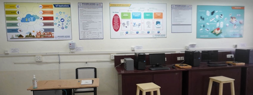
| Sl.No | Name of the Lab | Facility Available | Courses Offered | Virtual Link / ICT Tools | Soft copy of Lab Record |
|---|---|---|---|---|---|
| 1 | C Programming Lab | View Details | CS8261 - C Programming | View | Download |
| 2 | Internet Programming Lab | View Details | CS8661 - Internet Programming | View | Download |
| 3 | Operating Systems Lab | View Details | CS8461 - Operating Systems | View | Download |
| 4 | Object Oriented Analysis and Design Lab | View Details | CS8461 - Object Oriented Analysis and Design | View | Download |
| 5 | Web Technology Lab | View Details | IT8511 - Web Technology | View | Download |
| 6 | Networks Lab | View Details | CS8581 Networks Lab | View | Download |
Academics
Anna University Syllabus
| BE - 2021 Syllabus |
Course Materials
| S.No. | Subject Code | Subject Name | Lesson Plan | Question Bank | Lecture Notes | ICT Tools | |
|---|---|---|---|---|---|---|---|
| 1 | MA3354 | Discrete Mathematics | View | View | View | View | |
| 2 | CS3351 | Digital Principles and Computer Organization | View | View | View | View | |
| 3 | AD3391 | Database Design and Management | View | View | View | View | |
| 4 | AD3351 | Design and Analysis of Algorithms | View | View | View | View | |
| 5 | AD3301 | Data Exploration and Visualization | View | View | View | View | |
| 6 | AL3391 | Artificial Intelligence | View | View | View | View | |
| 7 | AD3381 | Database Design and Management Laboratory | View | View | View | View | |
| 8 | AD3311 | Artificial Intelligence Laboratory | View | View | View | View | |
| 9 | GE3361 | Professional Development | View | View | View | View | |
PLACEMENT DETAILS


NEWS & EVENTS
Student Activities
Members of Alumni Association
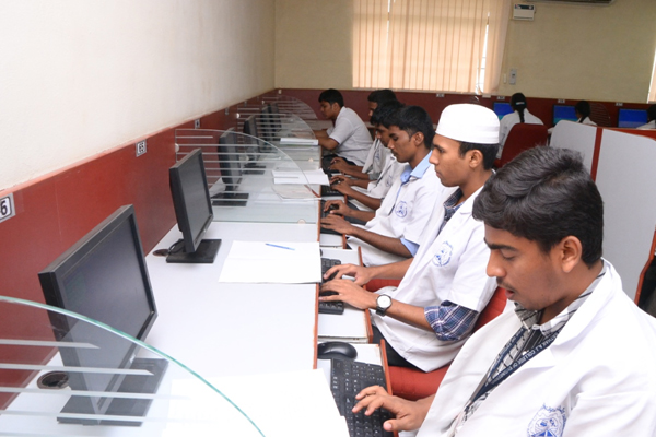
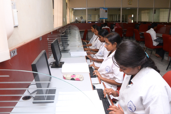
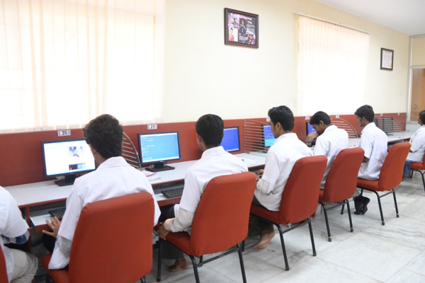
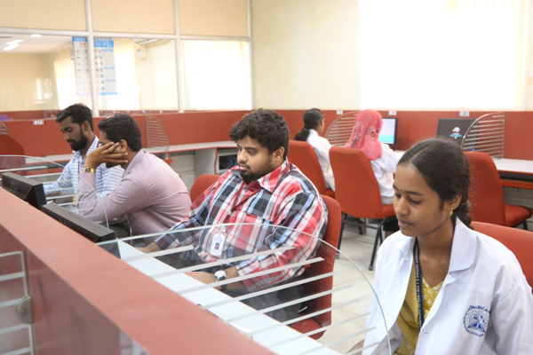
infrastructures